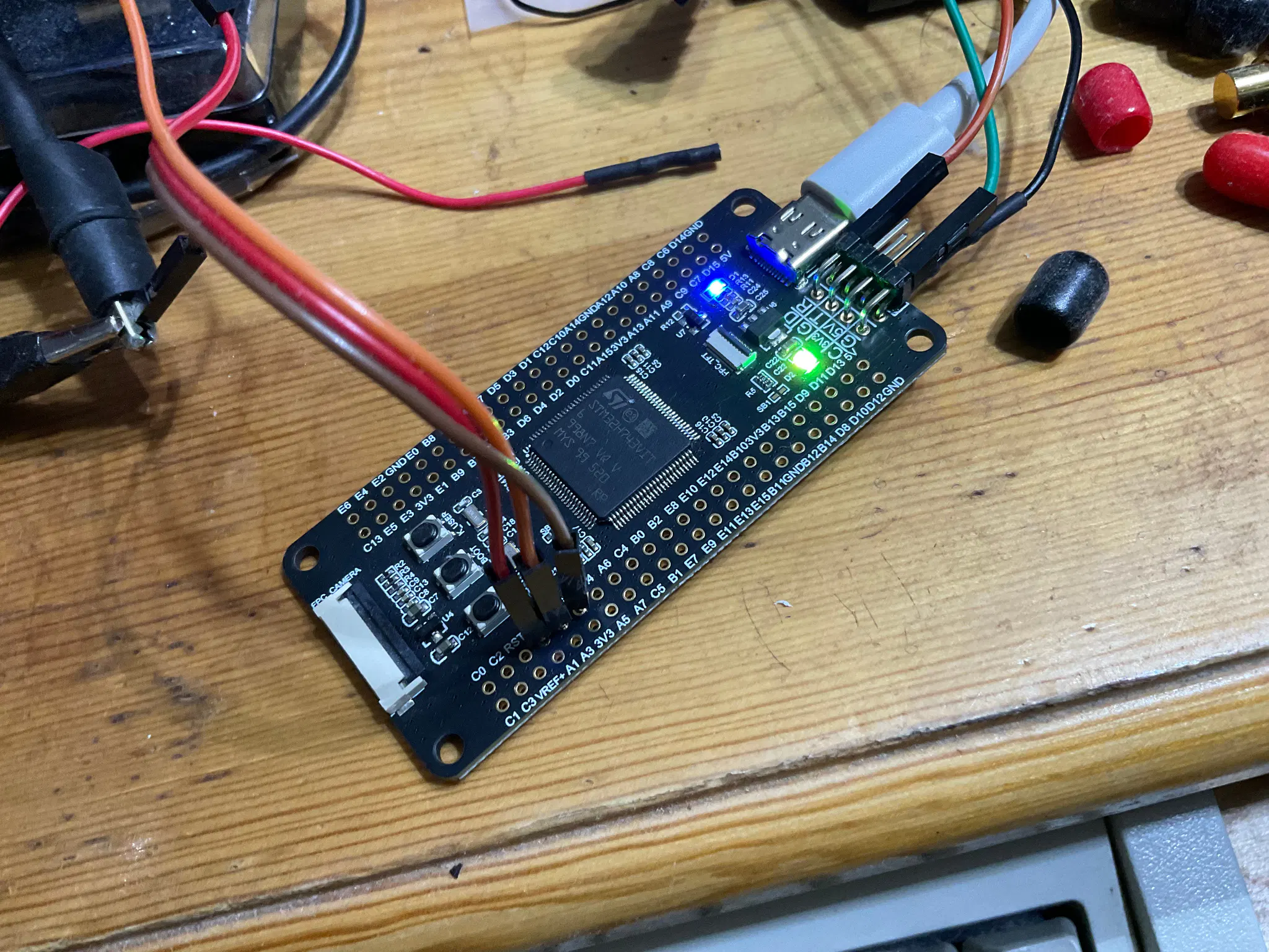
Optimizing IRQ latency on the STM32H743 @ 480 MHz, perhaps for NES ROM emulation...
-
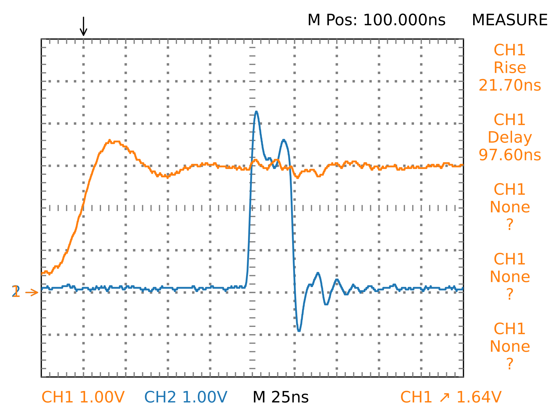
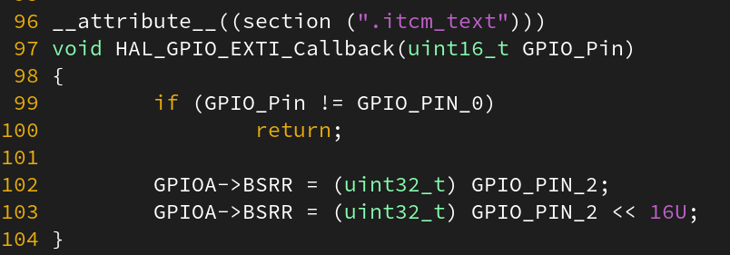
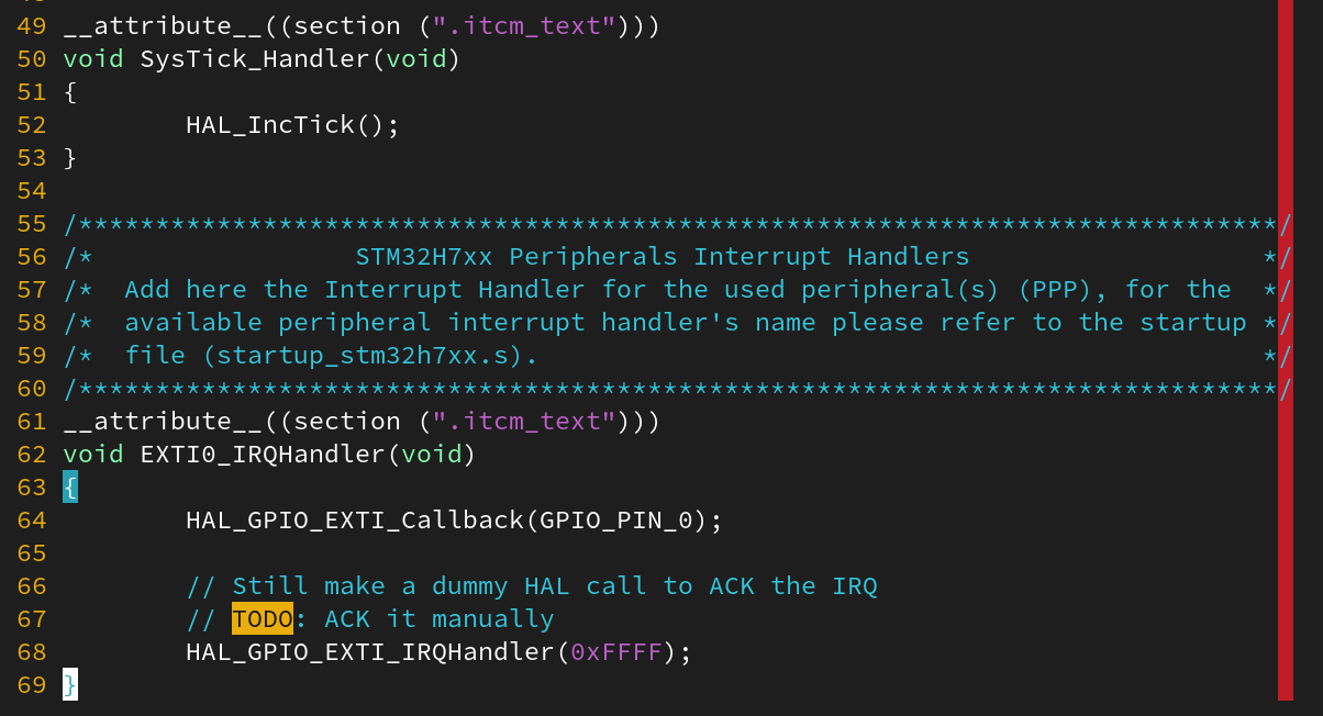
Optimizing IRQ latency on the STM32H743 @ 480 MHz, perhaps for NES ROM emulation... Best result so far: 100 nanoseconds input-to-output latency when the vector table and the IRQ handler are relocated to Tightly-Coupled Memory without making HAL calls. Not bad, but the GPIO controller (several buses away) looks like the real performance killer here. WARNING: buggy code, see correction https://mk.absturztau.be/notes/ajvb448y305b01i4. #electronics #STM32
Keep optimizing IRQ latency on the STM32H743 @ 480 MHz. Just enabled i-cache and d-cache, and the IRQ latency dropped from 100 ns to 70 ns.
 But cache shouldn't work like this. So my code is still touching slow memory somewhere. The stack perhaps, which is still in "normal" RAM. The slow Flash perhaps also makes it slower to abort
 main()if an instruction is stuck in a wait state. Need to check everything carefully... #electronics #STM32 -
Keep optimizing IRQ latency on the STM32H743 @ 480 MHz. Just enabled i-cache and d-cache, and the IRQ latency dropped from 100 ns to 70 ns.
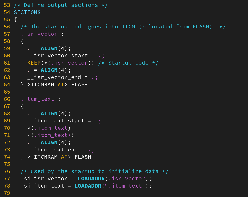
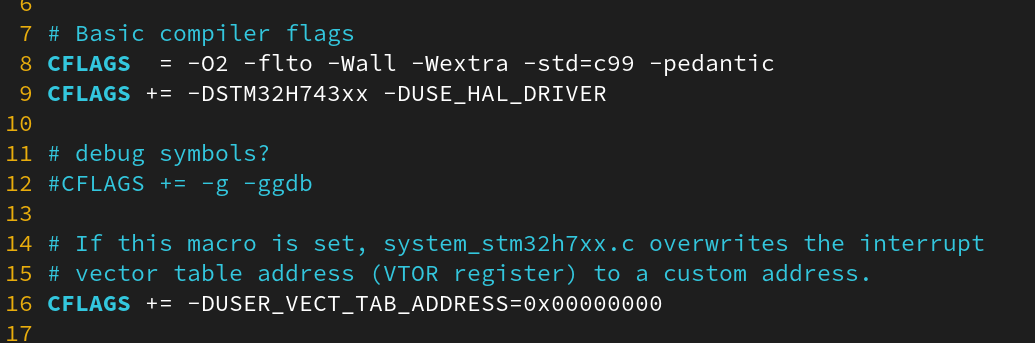
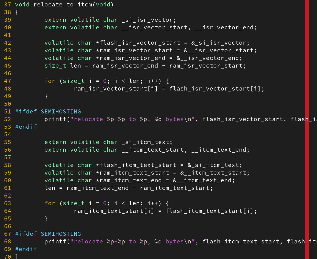
But cache shouldn't work like this. So my code is still touching slow memory somewhere. The stack perhaps, which is still in "normal" RAM. The slow Flash perhaps also makes it slower to abort main()if an instruction is stuck in a wait state. Need to check everything carefully... #electronics #STM32Keep optimizing IRQ latency on the STM32H743 @ 480 MHz. The 70 ns vs. 100 ns overhead mystery solved. I did not correctly relocate the vector table to Tightly-Coupled Memory properly, it was still in Flash. The STM32 HAL macro
USER_VECT_TAB_ADDRESSis a flag, not a memory address! In fact, only several hardcoded addresses are available, a real user override is not provided (the name "user" is a lie). Solution: just change VTOR manually, don't trust the startup code. I'm now getting 70-ns IRQ without CPU cache. #electronics #STM32 -
Keep optimizing IRQ latency on the STM32H743 @ 480 MHz. The 70 ns vs. 100 ns overhead mystery solved. I did not correctly relocate the vector table to Tightly-Coupled Memory properly, it was still in Flash. The STM32 HAL macro
USER_VECT_TAB_ADDRESSis a flag, not a memory address! In fact, only several hardcoded addresses are available, a real user override is not provided (the name "user" is a lie). Solution: just change VTOR manually, don't trust the startup code. I'm now getting 70-ns IRQ without CPU cache. #electronics #STM32 -
I do not understand how the NES system bus works, even after reading multiple tutorials. Only one way to find out... #electronics #NES #NESdev
Keep optimizing IRQ latency on the STM32H743 @ 480 MHz. I decided to try an event loop using the
WFEinstruction instead of IRQs, and I managed to get 60 ns input-to-output latency. I suspect this is the best possible latency. Latency did not improve by abusing QSPI controller to generate a write request (in fact it slightly degraded), even if the QSPI controller is physically close to the CPU. Clearly, passively monitoring signals is not the way to go for bus emulation. Perhaps the solution is predicting the clock before it even arrives, by internally generating a phase-shifted version of it. #electronics #STM32 -
Keep optimizing IRQ latency on the STM32H743 @ 480 MHz. I decided to try an event loop using the
WFEinstruction instead of IRQs, and I managed to get 60 ns input-to-output latency. I suspect this is the best possible latency. Latency did not improve by abusing QSPI controller to generate a write request (in fact it slightly degraded), even if the QSPI controller is physically close to the CPU. Clearly, passively monitoring signals is not the way to go for bus emulation. Perhaps the solution is predicting the clock before it even arrives, by internally generating a phase-shifted version of it. #electronics #STM32Keep optimizing IRQ latency on the STM32H743 @ 480 MHz. My "zero-latency IRQ" idea is a success, now I'm getting a 17.30 ns "effective" latency! Upon receiving every rising edge of the clock, the hardware immediately starts a timer that fires after a programmed delay, calculated to be slightly before the next clock rising edge. This way, the firmware is triggered from recovered, phase-shifted version of the clock, a little bit like how analog NTSC TVs got their H/VSYNC. Interrupt latency is completely eliminated for all but the first clock cycle (which is also predictable with pre-enabled outputs, since it's always the reset vector) Perfect bus emulation starts looking feasible. #electronics #STM32
-
Keep optimizing IRQ latency on the STM32H743 @ 480 MHz. My "zero-latency IRQ" idea is a success, now I'm getting a 17.30 ns "effective" latency! Upon receiving every rising edge of the clock, the hardware immediately starts a timer that fires after a programmed delay, calculated to be slightly before the next clock rising edge. This way, the firmware is triggered from recovered, phase-shifted version of the clock, a little bit like how analog NTSC TVs got their H/VSYNC. Interrupt latency is completely eliminated for all but the first clock cycle (which is also predictable with pre-enabled outputs, since it's always the reset vector) Perfect bus emulation starts looking feasible. #electronics #STM32
-
Making a 60-pin Famicom debug cartridge for testing my cartridge emulator... #electronics #NES #NESdev
"Warn : no flash bank found for address 0x08100000"
Spent half an hour trying to figure out why can't OpenOCD see my upper flash bank, while claiming my STM32 is dual-banked at the same time. Solution: usestm32h7x_dual_bank.cfg, notstm32h7x.cfg. #electronics #STM32
-
M monkee@other.li shared this topic
-
"Warn : no flash bank found for address 0x08100000"
Spent half an hour trying to figure out why can't OpenOCD see my upper flash bank, while claiming my STM32 is dual-banked at the same time. Solution: usestm32h7x_dual_bank.cfg, notstm32h7x.cfg. Still working on the same 60-pin Famicom cartridge emulator devboard. Finding a single-layer solution for the 480 MHz STM32H7 on a 2-layer power+signal / GND only stackup is like kicking a dead whale down the beach. I should've used a 4-layer board, but at least I now have the bragging right of developing the least radiative 2-layer PCB for the NES. #electronics #NES #NESdev
-
Still working on the same 60-pin Famicom cartridge emulator devboard. Finding a single-layer solution for the 480 MHz STM32H7 on a 2-layer power+signal / GND only stackup is like kicking a dead whale down the beach. I should've used a 4-layer board, but at least I now have the bragging right of developing the least radiative 2-layer PCB for the NES. #electronics #NES #NESdev
-
Still working on the same 60-pin Famicom cartridge emulator devboard. #electronics #NES #NESdev
EMC Pro Tip: rejoin the GND later nearby if you must split it, so the loop area doesn't go off the chart. P.S: I think a ground pour with vias should work even better here, as the signal traces would form coplanar waveguides with well-defined reference planes on the same layer. #electronics #NES #NESdev
-
EMC Pro Tip: rejoin the GND later nearby if you must split it, so the loop area doesn't go off the chart. P.S: I think a ground pour with vias should work even better here, as the signal traces would form coplanar waveguides with well-defined reference planes on the same layer. #electronics #NES #NESdev
The holy grail of 2-layer PCB is when you have just a metal sheet on layer 2. I think I'm quite close, but unfortunately some external jumpers are needed to finish the remaining control lines without cutting this beautiful plane. Even THT resistor jumpers are not enough to jump across the 24-trace bus. #electronics #NES #NESdev
-
The holy grail of 2-layer PCB is when you have just a metal sheet on layer 2. I think I'm quite close, but unfortunately some external jumpers are needed to finish the remaining control lines without cutting this beautiful plane. Even THT resistor jumpers are not enough to jump across the 24-trace bus. #electronics #NES #NESdev
NES quirk: the VRAM has two memory layouts that "wraps back" either horizontally or vertically for different scrolling games. This is called "nametable mirroring" mode, controlled by routing the raw "CIRAM A10" signal to the PPU A10/A11 address line via the cartridge port. But for my cartridge emulator, it means we're not just acting as a device sitting on the bus, it's actively messing with the PPU bus on the whole machine. Do I have enough time to do it in software GPIO, or do I have to use an external 2:1 hardware mux? Let's see:
* Hitachi HM6116 - Read: address valid prior to or coincident with /CS low. Write: address setup time 20 ns.
* Panasonic MN4216 - Read: address valid prior to or coincident with /CS low. Write: address setup time 20 ns.
* Sony CXK5816PN: Write: address setup time 0 ns.
* Sanyo LC3517: Write: address setup time 0 ns.
Conclusion: don't worry about it, "copy an address bus line 20 ns before /CS falls" is not a significant timing constraint to the existing 180 ns budget for the emulator. #electronics #NES #NESdev -
oof.
 #electronics #NES #NESdev
Downsized all input resistors from 1206 to 0603, preparing to use the extra space for more air bridges. I initially switched from 0603 to 1206 to give space for horizontal traces, but I found it did not really have any advantage in comparison to 0603, as the vertical traces blocked all the horizontal ways anyway, 0603 + selective 1206 jumpers probably can solve this deadlock. #electronics #NES #NESdev
-
Downsized all input resistors from 1206 to 0603, preparing to use the extra space for more air bridges. I initially switched from 0603 to 1206 to give space for horizontal traces, but I found it did not really have any advantage in comparison to 0603, as the vertical traces blocked all the horizontal ways anyway, 0603 + selective 1206 jumpers probably can solve this deadlock. #electronics #NES #NESdev
Unfortunately the original layout couldn't be completed because the placement and fan-out were not designed with "single-layer flowthrough" in mind, as I originally had no idea about the pinout. The whole board layout was thus abandoned and restarted. Now I have a 99% zero-gap ground plane, with only 13 non-perpendicular cuts under the connectors without interrupting GND. An army of 0-ohm jumpers bridge signals to human-friendly positions. #electronics #NES #NESdev
-
Almost finished my Famicom cartridge devboard. This time all signals fanned out successfully under the 2-layer + "Zero Gap" ground plane constraints. 100 MHz signal integrity disciplines applied to a 1 MHz bus. #electronics #NES #NESdev
@niconiconi@mk.absturztau.be I don't understand half of it and love it! Thanks for sharing